How does a transistor work?🙄...
Transistors... How do they work?...

It is one of the most important devices ever to be invented. So, we're going to learn how do they work in detail in here.
What is a transistor?
Transistors come in many shapes and sizes. There are two main types, the bipolar and the field effect.
We're going to mostly focus on the bipolar version.

Transistors are small electronic components with two main functions. It can act as a switch to control circuits and they can also amplify signals.
Small low power transistors are enclosed in a racing case to help protect the internal parts. But higher power transistors will have a partly metal case, which is used to help remove the heat which is generated as this will damage the components over time.

We usually find these metal body transistors attached to a heat sink, which helps remove the unwanted heat. For example, inside this circuit
We have some mosfet transistors which are attached to very large heat sinks.
Without the heat sink the components quickly reach 45 degrees Celsius or 113 degrees Fahrenheit. With a current of just 1.2A.
They will become much hotter as the current increases. But for electronic circuits with small currents, we can just use these resin body transistors which do not require a heat sink.
On the body of the transistor. We find some text.

This will tell us the part number which we can use to find the manufacturers datasheet. Each transistor is rated to handle a certain voltage and current, so it is important to check these sheets. Now with the transistor we have three pins labelled E, B and C.
This stands for the emitter, the base and the collector. Typically with these resin body type TRANSISTORS with a flat edge, the left pane is the emitter, the middle is the base, and the right side is the collector.

However, not all transistors use this configuration. So do check the manufacturer’s datasheet.

We know that if we connect a light bulb to a battery, it will illuminate. We can install a switch into the circuit and control the light by interrupting the power supply. But this requires a human to manually control the switch.
So how can we automate this?
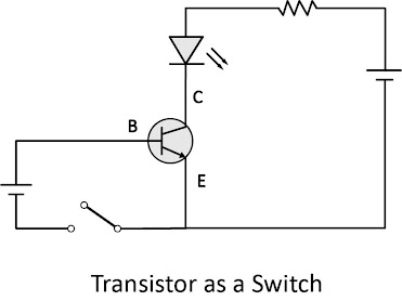 For that, we use a transistor. This transistor is blocking the flow of current. So the light is off. But if we provide a small voltage to the base pane in the middle, it causes the transistor to start allowing current to flow in the main circuit. So the light turns on.
We can then place a switch
on the controlling pin to operate it remotely or we can place a sensor on this to automate the control. Typically, we need to apply at least 0.6V to 0.7 volts to the base pin for the transistor to turn on. For example, this simple transistor circuit has a LED and a nine volt power supply across the main circuit. The base pin is connected to the DC Bench power supply. The circuit diagram looks like this.


When the supply voltage to the base pin is 0.5V the transistor is off. So the LED is also off at 0.6V the transistor is on, but not fully. The LED is dim because the transistor is not yet letting the full current flow through the main circuit. Then at 0.7V the lead is brighter because the transistor is letting almost the full current through. At 0.8V, the LED is at full brightness. The transistor is fully open. So what's happening is we're using a small voltage and current to control a larger voltage and current.

The collector has a much higher current, for example, 100mA. The ratio between these two is known as the current gain and uses the symbol beta (β).
We can find the ratio in the manufacturer’s datasheet. In this example, the collector current is 100mA and the base current is 1mA. So the ratio is 100mA divided by 1mA, which gives us 100. We can also rearranges formula to find the currents also.
 Transistors are shown on electrical drawings with symbols like these, the arrow is placed on the emitter. The arrow points in the direction of conventional current so that we know how to connect them into our circuits.
 How does a transistor work?
To understand how a transistor works, I want you to first imagine water flowing through a pipe. It flows freely through the pipe until we block it with a disc. Now, if we connect a smaller pipe into the main one and place a swing gate within this small pipe, we can move the disc using a pulley. The further the swing gate opens, the more water is allowed to flow in the main pipe. The swing gate is a little heavy, so a small amount of water won't be enough to open it.
A certain amount of water is required to force the gate to open. The more water we have flowing in this small pipe, the further the valve opens and allows more and more water to flow in the main pipe.
This is essentially how an NPN transistor works. You might already know that when we design electronic circuits, so in this NPN transistor circuit, we assume that the current is flowing from the batteries positive into both the collector and the base pin and then out of the emitter pin. We always use this direction to design our circuits.
However, that's not what's actually occurring. In reality, the electrons are flowing from the negative to the positive of the battery. This was proved by Joseph Thompson, who carried out some experiments to discover the electron and also prove they flowed in the opposite direction. So in reality, electrons flow from the negative into the emitter and then out of the collector and the base pin. We call this electron flow.
Remember, we always design circuits using the conventional current method. But scientists and technologists know that electron flow is how it actually works by the way.

So we know that electricity is the flow of electrons through a wire. The copper wire is the conductor and the rubber is the insulator. Electrons can flow easily through the copper, but they can't flow through the rubber insulator. If we look at this basic model of an atom of a metal conductor, we have the nucleus at the Centre and this is surrounded by a number of orbital shells which hold the electrons. Each shell holds a maximum number of electrons, and an electron needs to have a certain amount of energy to be accepted into each shell.
The electrons located furthest away from the nucleus hold the most energy. The outermost shell is known as the valence shell. A conductor has between one and three electrons in its valence shell. The electrons are held in place by the nucleus, but there is another shell known as the conduction band.
If an electron can reach this, then it can break free from the atom and move to other atoms. With a metal atom such as copper. The valence shell and the conduction band overlap, so it's very easy for the electrons to move with an insulator the outermost shell is packed. There's very little to no room for an electron to join. The nucleus has a tight grip on the electrons and the conduction band is far away. So the electrons can't reach this to escape. Therefore, electricity cannot flow through this material.
However, there's another material known as a semiconductor. Silicon is an example of a semiconductor. With this material, there's one too many electrons in the valence shell for it to be a conductor. So it acts as an insulator. But as the conduction band is quite close, if we provide some external energy, some electrons will gain enough energy to make the jump into the conduction band and become free. Therefore, this material can act as both an insulator and a conductor.
Pure silicon has almost no free electrons. So what technologists do is dope the silicon with a small amount of another material which changes its electrical properties.
We call this P type and N type doping. We combine these materials to form the PN junction. We can sandwich these together to form an NPN or PNP transistor. Inside the transistor we have the collector pin and the emitter pin between these in an NPN transistor, we have two layers of N type material and one layer of P type. The base wire is connected to the P type layer in a PNP transistor this is just configured the opposite way. The entire thing is enclosed in a resin to protect the internal materials.
Let's imagine the silicon hasn't been doped yet, so it's just pure silicon inside. Each silicon atom is surrounded by four other silicon atoms. Each atom wants eight electrons in its valence shell but the silicon atoms only have four electrons in their valence shell, so they sneakily share an electron with their neighboring atom to get the 8 desire.
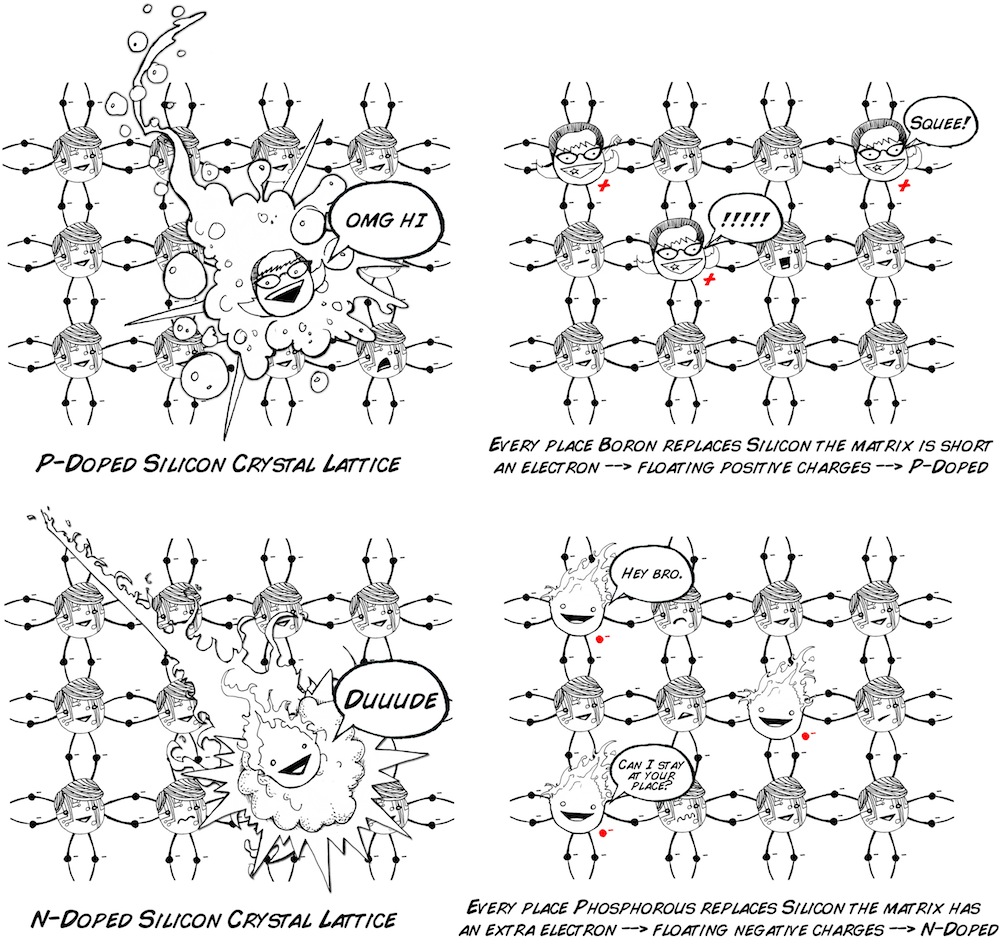
This is known as covalent bonding. When we add the N type material such as phosphorus, it will take the position of some of the silicon atoms. The phosphorus atoms have five electrons in their valence shell.
So as the silicon atoms are sharing electrons to get their desired eight, they don't need this extra one, which means there's now extra electrons in the material and these are free to move around with P type doping we add in a material such as aluminum.
This atom has only three electrons in this valence shell. It therefore can't provide its four neighbors with an electron to share. So one of them will have to go without. This means a hole has been created where an electron can sit and occupy.
We now have two doped pieces of silicon, one with too many electrons and one we not enough electrons. The two materials join to form a PN junction. At this junction we get what's known as a depletion region in this region some of the excess electrons from the N side will move over to occupy the holes in the P side. This migration will form a barrier with a buildup of electrons and holes on opposite sides.

The electrons are negatively charged and the holes are therefore considered positively charged, so this Build-Up causes a slightly negatively charged region and a slightly positively charged region. This creates an electric field and prevents more electrons from moving across. The potential difference across this region is typically around 0.7V when we connect a voltage source across the two ends with the positive connected to the P type material. This will create a forward bias and the electrons will begin to flow. The voltage source has to be greater than the 0.7V barrier. Otherwise, electrons cannot make the jump when we reverse the power supply so that the positive is connected to the N type material.
The electrons held in the barrier will be pulled back towards the positive terminal and the holes will be pulled back towards the negative terminal. This has caused a reverse bias in a NPN transistor. We have two layers of N type material, so we have two junctions and therefore two barriers, so no current can flow through it ordinarily. The emitter N type material is heavily doped, so there are a lot of excess electrons here. The base P type is lightly doped, so there are a few holes here. The collector N type is moderately doped, so there are a few excess electrons here.
If we connect a battery across the base and the emitter with the positive connected to the P type layer, this will create a forward bias. The forward bias causes the barrier to collapse as long as the voltage is at least 0.7V. So the barrier diminishes and the electrons rush across to fill the space within the P type material. Some of these electrons will occupy a hole and they will be pulled towards the positive terminal of the battery.
The P type layer is thin and was lightly doped on purpose so that there is a low chance of electrons falling into a hole. The rest will remain free to move around the material. Therefore, only a small current will flow out of the base pin, leaving an excess of electrons in the pinot material if we then connect another battery between the emitter and the collector with the positive connected to the collector, the negatively charged electrons within the collector will be drawn to the positive terminal, which causes a reverse bias.
 If you remember, with the reverse bias, the electrons and holes of the barrier are pulled back across, so the electrons on the P type side of the barrier are pulled across to the N type side and the holes on the N type side are pulled back to the P type side. They are already an excess number of electrons in the P type material.
So they will move to occupy these holes and some of them will be pulled across because the voltage of this battery is greater. So the attraction is much higher. As these electrons are pulled across, they flow into the battery. So a current develops across the reverse bias junction.

A higher voltage on the base pin fully opens the transistor, which means more current and more electrons moving into the P type layer. Therefore, more electrons are pulled across the reverse bias. We also see more electrons flowing in the emitter side of the transistor compared to the collector side.


Comments